| Resolution (Bits) | 16 |
| Number of DAC channels (#) | 1 |
| Interface type | SPI |
| Output type | Unbuffered Voltage |
| Settling time (μs) | 1 |
| Reference type | Ext |
| Architecture | R-2R |
| Rating | Catalog |
| Output range (Max) (mA/V) | 5.5 |
| Output range (Min) (mA/V) | 0 |
| Operating temperature range (C) | -40 to 85 |
- 16-Bit Resolution
- 2.7 V to 5.5 V Single-Supply Operation
- Very Low Power: 15 μW for 3 V Power
- High Accuracy, INL: 1 LSB
- Low Noise: 10 nV/
 Hz
Hz - Fast Settling: 1.0 μS
- Fast SPI? Interface, up to 50 MHz
- Reset to Zero-Code
- Schmitt-Trigger Inputs for Direct Optocoupler Interface
- Industry-Standard Pin Configuration
- APPLICATIONS
- Portable Equipment
- Automatic Test Equipment
- Industrial Process Control
- Data Acquisition Systems
- Optical Networking
SPI, QSPI are trademarks of Motorola, Inc.
Microwire is a trademark of National Semiconductor Corp.
All other trademarks are the property of their respective owners.
The DAC8830 and DAC8831 are single, 16-bit, serial-input, voltage-output digital-to-analog converters (DACs) operating from a single 3 V to 5 V power supply. These converters provide excellent linearity (1 LSB INL), low glitch, low noise, and fast settling (1.0 μS to 1/2 LSB of full-scale output) over the specified temperature range of -40°C to +85°C. The output is unbuffered, which reduces the power consumption and the error introduced by the buffer.
These parts feature a standard high-speed (clock up to 50 MHz), 3 V or 5 V SPI serial interface to communicate with a DSP or microprocessor.
The DAC8830 output is 0 V to VREF. However, the DAC8831 provides bipolar output (±VREF) when working with an external buffer. The DAC8830 and DAC8831 are both reset to zero code after power up. For optimum performance, a set of Kelvin connections to external reference and analog ground input are provided on the DAC8831.
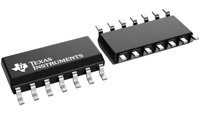
The DAC8830 is available in an SO-8 package, and the DAC8831 in an SO-14 package. Both have industry standard pinouts. The DAC8831 is also available in a QFN-14 package.


